Knowledge
Understanding Wafer Connector Terminal Structure and Design
The wafer connector terminal consists of a male and a female side that are designed to interlock and create a secure electrical connection. The male side of the connector contains a set of pins or blades that are designed to fit into the female side of the connector. The female side contains a corresponding set of contact points or sockets that are designed to receive the pins or blades of the male side.
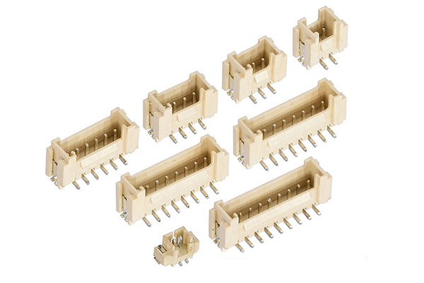
In semiconductor and microelectronic systems, the wafer connector terminal stands as one of the most critical yet often overlooked components. Serving as the physical and electrical bridge between silicon wafers and external circuits, its structure and design directly determine connection reliability, signal integrity, and overall device performance—especially as devices shrink and packaging density rises.
At its core, the terminal is engineered to meet dual demands: precise mechanical alignment and stable electrical transmission. Structurally, it typically consists of three key zones: the contact interface that bonds or presses against the wafer, the transitional support section, and the lead-out end that connects to substrates or packaging lines. The contact region is carefully shaped—often with a specific curvature or tapered profile—to ensure uniform pressure distribution, minimizing contact resistance while avoiding damage to delicate wafer surfaces. Material selection goes hand in hand with form: high-conductivity alloys or plated metals balance electrical conductivity with mechanical spring properties, ensuring consistent contact over thousands of assembly cycles and wide temperature ranges.
Design considerations extend far beyond basic shape and conductivity. Thermal expansion matching between the terminal and the wafer is critical; mismatched coefficients can introduce stress that leads to warping, contact failure, or even cracking under operational temperature swings. Structural rigidity is calibrated to avoid excessive deflection while maintaining enough compliance to accommodate minor dimensional variations in wafers and packaging. Surface finish and coating—such as gold or palladium plating—are integral design choices that reduce oxidation, lower contact resistance, and extend service life in harsh environments.
Every dimension, angle, and material layer is refined for a specific purpose: supporting high-frequency signal transmission without distortion, withstanding mechanical vibration, and enabling automated, high-precision assembly. In short, the wafer connector terminal's structure and design are not merely mechanical details—they are foundational to unlocking the full performance potential of modern microelectronics.
RELATED NEWS
- Why Do Customers Prefer Right Angle LED Tact Switch 2026-08-24
- Why Choose Metal Push Button Switches with Pre-Wired Cable 2026-07-28
- Why Do Customers Choose Wired Metal Push Button Switches 2026-06-24
- What is a metal push button switch used for 2026-05-19
- The most common problems with DIP switches 2026-04-01
CATEGORIES
LATEST NEWS
CONTACT US
Contact: Bella
Phone: 15999819066
E-mail: rucoe@rucoe.com
Whatsapp:+86-15999819066
Add: Taoyuan Street, Nanshan, Shenzhen